
Research
Introduction: Atomic-Scale View of Interfacial Processes with X-rays
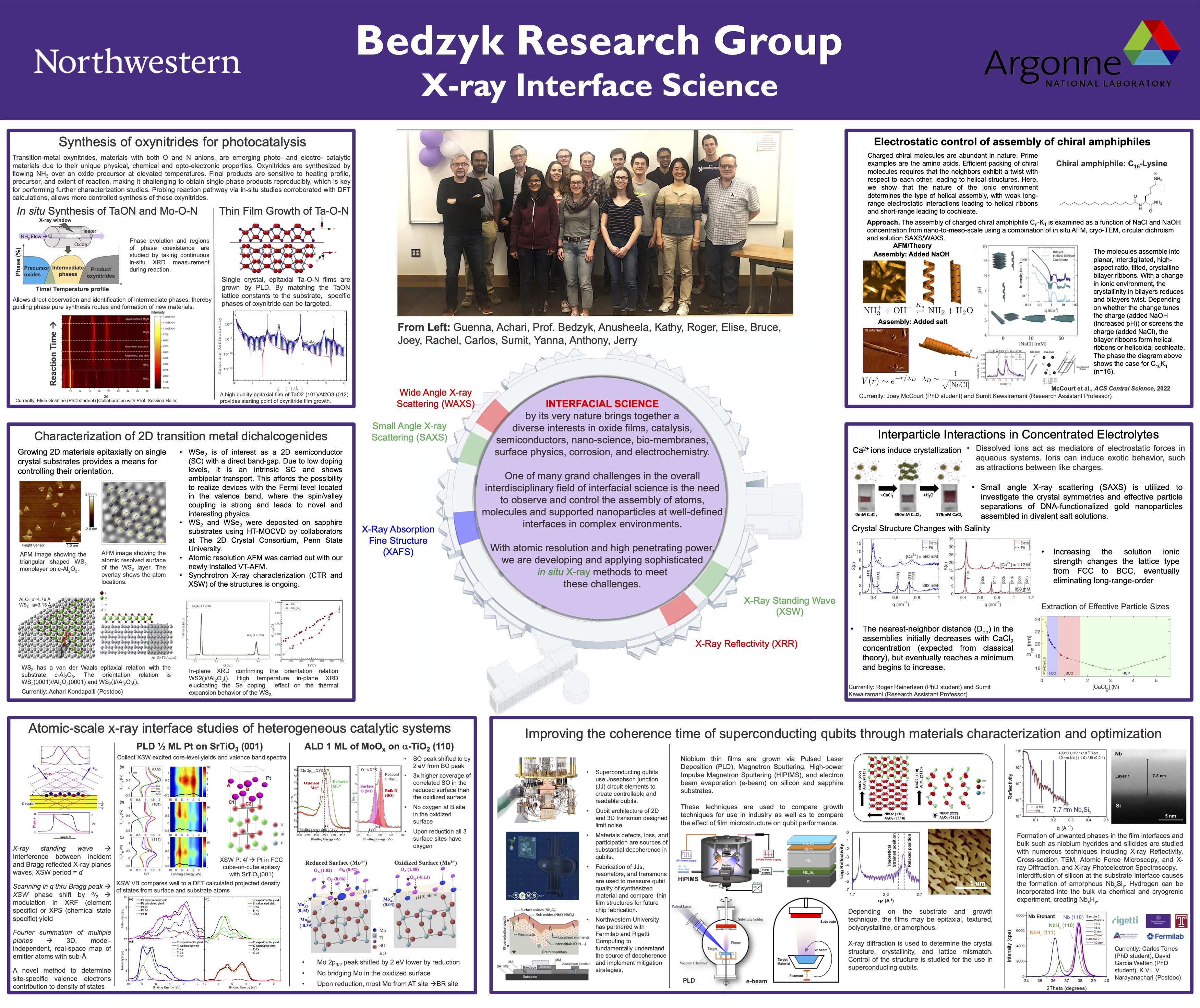
Oxygens on α-TiO2(110)
Our research program includes the development of novel X-ray probes and the characterization of surface, interface, and thin-film structures with atomic resolution. We conduct our experiments using both in-house and synchrotron X-ray facilities. The latter have greatly enhanced chemical and structural sensitivity for studying systems as dilute as one-hundredth of an atomic monolayer.
In addition to using more conventional X-ray scattering and spectroscopy techniques, we have developed a number of methods for generating X-ray standing waves with differing characteristic length scales. We use these periodic X-ray probes to pinpoint the lattice location of adsorbate atoms on crystalline surfaces, to measure strain within epitaxially grown semiconductor and ferroelectric thin films, and to locate heavy atoms within ordered ultrathin organic films.
Using a state-of-the-art surface science facility at the Advanced Photon Source, we perform in situ analysis of surface structures and phase transformations of MBE-grown ordered atomic monolayers on semiconductor and complex oxide surfaces. We also use X-ray standing waves, high-resolution X-ray diffraction, and X-ray absorption spectroscopy for structural characterization of buried strained-layer semiconductor heterostructures, ferroelectric thin films and the water/crystalline interface.
Research Highlights
X-ray Scattering and Spectroscopy Studies of Interface Structure of Supported 2D Nanocrystals
The surface termination of the underlying substrate support and reconstruction at the support - over layer interface play a significant role for the functional aspects of the 2D system. Knowledge of such a buried interface structure, both atomically and chemically, is crucial to understand their impact on electronic, optical, sensing and catalytic applications.
Some examples:
Refs:
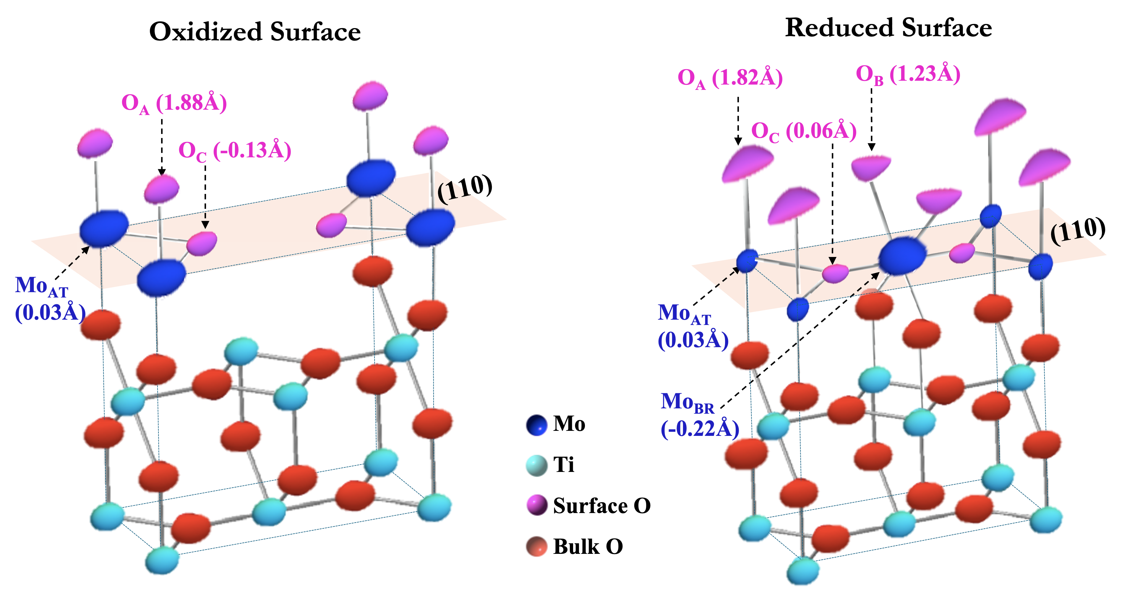
[1] G. P. Campbell, A. J. Mannix, J. D. Emery, T.-L. Lee, N. P. Guisinger, M. C. Hersam, and M. J.
Bedzyk, Resolving the Chemically Discrete Structure of Synthetic Borophene Polymorphs,Nano Lett.
18, 2816-2821 (2018).
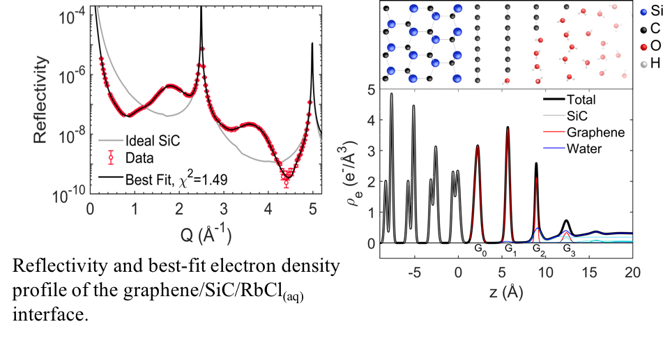
[2] J. D. Emery, B. Detlefs, H. J. Karmel, L. O. Nyakiti, D. Kurt Gaskill, M. C. Hersam, J. Zegenhagen,
and M. J. Bedzyk, Chemically Resolved Interface Structure of Epitaxial Graphene on SiC(0001), Phys. Rev.
Lett., 111, 215501 (2013)
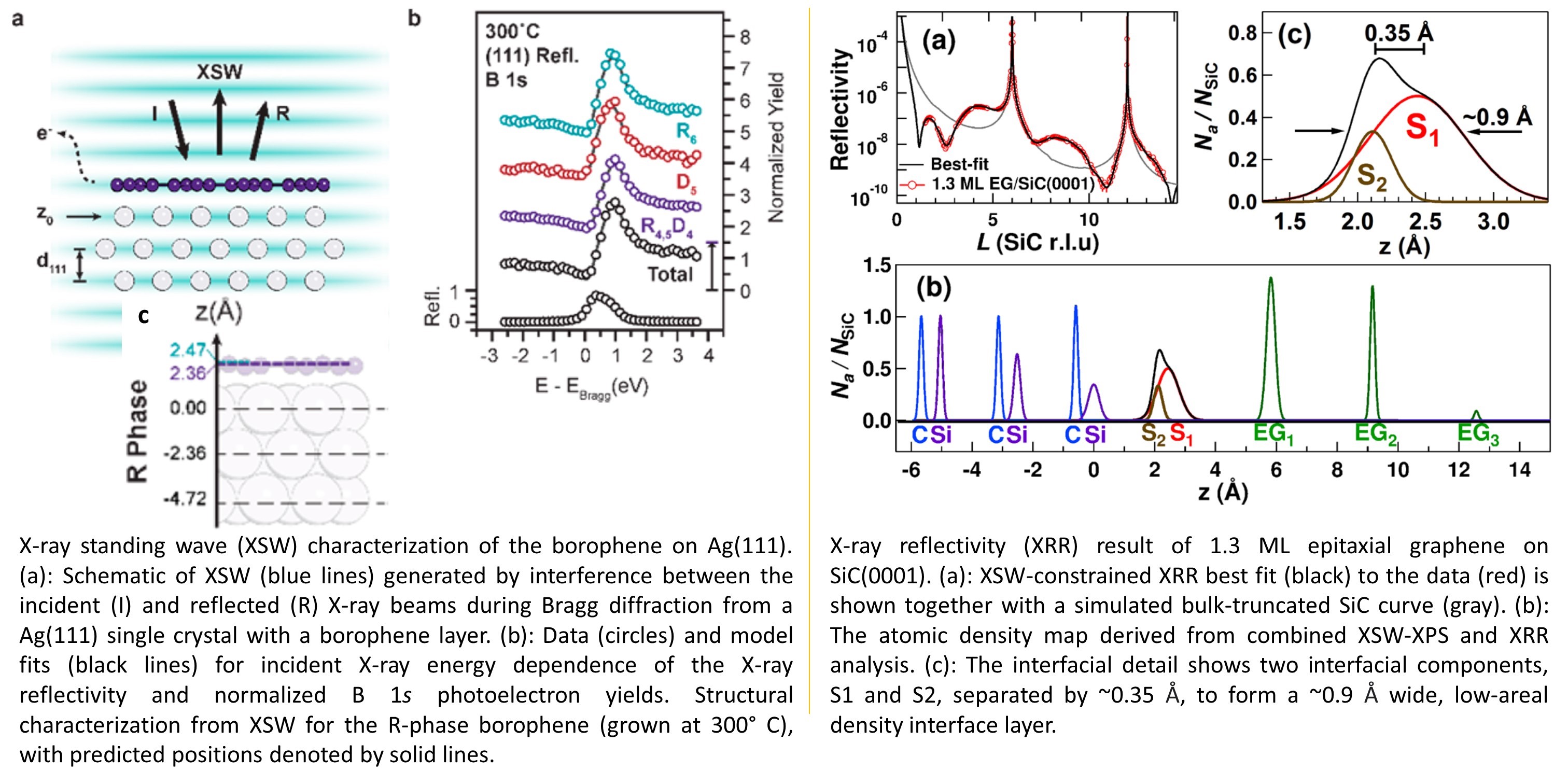
Polymorphism in Peptide Amphiphile Assemblies
Peptide amphiphiles (PA) can assemble in a variety of morphologies. To understand how electrostatics drives the transformation in morphology and molecular packing, we studied the assembly of a charge-tunable (via pH) ionic PA by a combination of solution small and wide angle X-ray scattering (SAXS/WAXS), cryo-transmission electron microscopy (Cryo-TEM) and Monte-Carlo simulations.
Ref: Gao, C. Olvera de la Cruz. M., Bedzyk, M. J., J. Phys. Chem. B 121, 1623-1628 (2017)
Ion Adsorption at Charged Solid-Aqueous Interfaces
Capacitive energy storage is driven by adsorption of ions at an electrode-electrolyte interface. In-situ X-ray reflectivity (XR) and anomalous XR can help elucidate the adsorbed ion structure and underlying phenomena that give rise to observed structures.
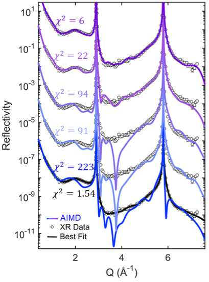
Direct, quantitative comparison between X-ray reflectivity and theory highlights important structural differences between the two methods and helps guide further development of predictive computational tools.
Ref: Harmon, K., Chen, Y., Bylaska, E., Catalano, J., Bedyzk, M., Weare, J., Fenter, P. J. Phys. Chem. C, 122, 47, 26934-26944
Counterion Distribution Surrounding Protein-DNA Conjugates
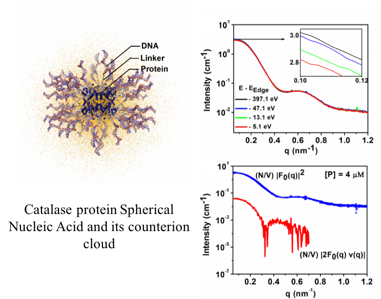
The charge compensating counterionic cloud surrounding Protein Spherical Nucleic Acid conjugates strongly mediates its structure and function. Here Anomalous Small Angle X-ray scattering and DFT are used to elucidate the structure of the Rb+ ion cloud and DNA shell surrounding the conjugate with nanometer-scale resolution.
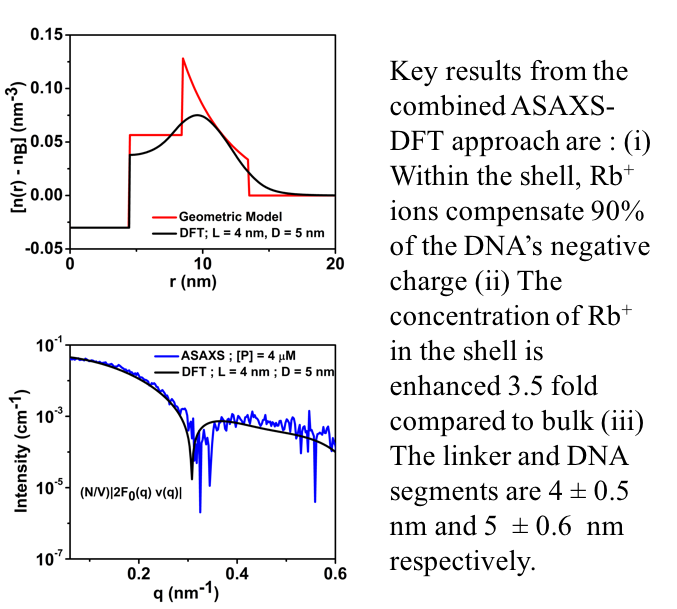
Ref: Krishnamoorthy, K., ACS Cent. Sci., 2018, 4 (3), pp 378-386
The Beam Team
Source: Northwestern Magazine
at Argonne National Laboratory near Lemont, IL.
Photoclip from Northwestern Magazine WINTER 2014.
Courtesy of Argonne National Laboratory.
At the Advanced Photon Source, Northwestern researchers use extremely bright X-rays to do atomic-level basic research that is critical to the creation of new drugs, innovative catalysts, better batteries and new sources of energy.
“....These are the brightest, most intense X-rays available in the Western Hemisphere,” says Michael Bedzyk, professor of materials science and engineering at the McCormick School of Engineering and Applied Science and co-director of the Northwestern Synchrotron Research Center. Bedzyk’s own group uses the X-rays to explore how atoms align at the interfaces that separate two different materials...."
Catalysts Caught in the Act Undergo Radical Rearrangements During Reactions
Source: SCIENCE AND RESEARCH HIGHLIGHTS of Advanced Photon Source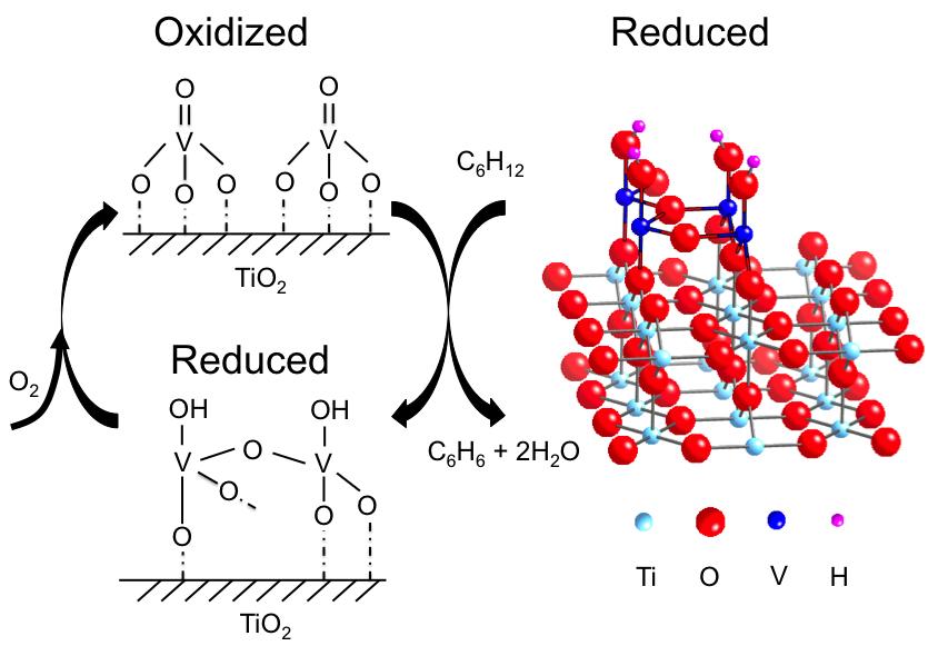
The atomic-scale structure and chemical properties of catalysts remain surprisingly mysterious, despite the critical roles that catalysts play in a variety of industrial and environmental applications. Researchers working at the U.S. Department of Energy Office of Science's Advanced Photon Source teased out structural and chemical information about a single layer of vanadium oxide, a catalyst, supported on the surface of a titanium oxide crystal, making it possible for scientists to improve catalysts by strategically altering their structures.
Atomic-Scale Study of Ambient-Pressure Redox-Induced Changes for an Oxide-Supported Submonolayer Catalyst: VOx/α-TiO2(110)
Source: ACS Live Slides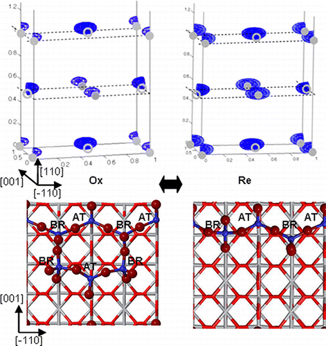
These slide presentations are created by Zhenxing Feng about his published research in the Journal of Physical Chemistry Letters, and include his own voice describing the research as the slides automatically advance. Please listen to Zhenxing telling you an interesting story about "Atomic-Scale Study of Ambient-Pressure Redox-Induced Changes for an Oxide-Supported Submonolayer Catalyst: VOx/α-TiO2(110)"